
Test grating TGG1 is intended for:
- SPM calibration in X or Y axis;
- detection of lateral and vertical scanner nonlinearity;
- detection of angular distortion;
- tip characterisation
Grating description
|
Structure: |
the grating is formed on Si wafer top surface |
|
Pattern types: |
1- D array of triangular steps (in X or Y direction) having precise linear and angular sizes |
|
Edge angle: |
70 degrees |
|
Edge radius: |
≤10nm |
|
Period: |
3±0,05µm |
|
Chip size: |
5x5x0,5mm |
|
Effective area: |
central square 3x3mm |
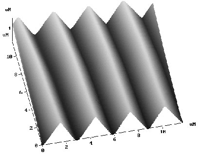
Fig.1 SPM image of TGG1 grating